Instrumentation and Measurement & Lab – Week #2 Lecture 1
Overview
2.1 Introduction
Computers are digital electronic devices, so all the
information they work with must be digitally formatted. Digital electronics has
given us the power to accurately control extremely complex processes that were
beyond our wildest dreams a few years ago [1]. It would take many volumes to
cover the subject of digital technology, so in this text we can only scratch
the surface. There is a place for both analog and digital circuits in
instrumentation.
Sensors and instrumentation functions are analog in nature.
However, digital circuits have many advantages over analog circuits. Analog
signals are easily converted to digital signals using commercially available
analog to digital converters (ADC). In new designs, digital circuits will be
used wherever possible.
Some of the advantages of digital circuits are:
·
Lower power requirements;
·
Increased cost effectiveness;
·
Ability to control multivariable systems
simultaneously;
·
Ability to transmit signals over long distances
without loss of accuracy and elimination of noise;
·
Higher speed signal transmission;
·
Memory capability for data storage;
·
Compatibility with controllers and alphanumeric
displays.
2.2 Review of Digital Fundamentals
A summary of basic digital electronics concepts is presented
in appendix 2.
2.2.1 Digital information
The use a digital techniques and process control requires
that process variable measurements and control information be encoded into
digital form. The digital form may be represented in many ways, such as two
voltages, two frequencies, or two phases. The digital information is usually
represented as a high state or 1 or a low state or 0 on a wire that carries the
digital signal.

Digital Words
An assemblage of digital levels to construct a binary number
is often called a word. The individual digital levels are referred to as bits
of the word. A 6 bit word consists of six independent
levels or six bits, consisting of ones or zeros.
Decimal Whole Numbers
Refer to Appendix 2 and the examples for conversion of
decimal numbers to binary and from binary to their equivalent, based 10 value.
Octal and Hex Numbers
Decimal numbers can also be represented as base 8 numbers,
also known as octal and hexadecimal.
2.2.2 Fractional Binary Numbers
Binary numbers can also represent decimal floating
point numbers. Reference appendix 2 and the examples.
2.2.3 Boolean Algebra
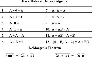
Boolean algebra is a mathematical procedure that allows the
combinations of true or false conditions in various logical operations by
equations so that conclusions may be drawn. The fundamentals of Boolean algebra
are also summarized in the table below.
2.2.4 Digital Electronics
The electronic building blocks of digital electronics are
designed to operate on the binary levels present on digital signal lines. The
basic structure involves the use of AND/OR logic and NAND/NOR logic.
2.2.5 Programmable Logic Controllers
An outgrowth of digital electronics and computers and
industrial control resulted in the creation of special controllers called
programmable logic controllers or PLCs. These devices are particularly suited
to the solution of control problems associated with Boolean equations and
binary logic problems in general. PLCs now directly replace relays and
mechanical sequence controllers.
2.2.6 Computer Interface
The term interface refers to the hardware connections and
software operations necessary to input and output data using connections to a
computer. Typically, data lines, address lines and control lines are necessary
to carry digital information.
Tri-buffers state
Tri-state buffers allow multiple signals to share a single
digital line on a bus.
2.3 Converters
We live in an analog world and sensor measurements are
analog in nature. All of our computational functions, signal transmission, data
storage, signal conditioning, and so forth, derive many benefits from the
digital world. It is therefore necessary to convert our analog signals into a
digital format for processing, and then back to analog for final control. The
interface between the analog world and digital world uses converters. An ADC
changes the analog signal into a digital format, and a DAC changes the digital
signal back to analog. The characteristics of these converters must be precise
and accurately known, to establish the relationship between the analog and
digital signal.
2.3.1 Comparators
The simplest form of information transfer between an analog
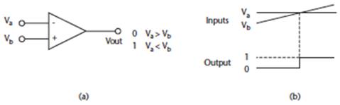
signal and a digital signal is a comparator. This device is simply a high gain
amplifier that is used to compare two analog voltages, and depending on which
voltage is larger, will give a digital “0” or “1” signal. This device is shown
in the figure below (a), with the input and output waveforms in figure (b). The
comparator is an integral part of ADCs and DACs, and of many monitoring
devices.
One of the input voltages in this case, Va,
is known as a fixed trigger level, a set level, or a reference voltage. The
other voltage is the variable, which when compared to Va
in a comparator, will give a digital “1” or “0” signal, depending on whether it
is greater than or less than the reference voltage.
Open-Collector Comparators
An open-collector output from a comparator can be used with
a pull-up resistor to directly produce a voltage level equal to a one or zero.
It is possible to directly drive a relay or use multiple comparators ORed together to provide an output.
Hystersis Comparator
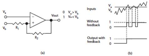
Hysteresis is obtained with positive feedback, as shown in
figure (a), and is often used in comparators to minimize or overcome noise
problems. Some noise can be filtered out, but it is difficult to completely
eliminate all of it. Noise can cause the comparator to switch back and forth,
giving uncertainty in the trigger point. This is shown in figure below (b),
where input Vb is varying as it increases due to
noise. This input, when used in a comparator without feedback, gives several
“1” level outputs as shown, which may cause problems when trying to interpret
the signal. If positive feedback (or hysteresis) is used, as shown in figure
below (a), then a clean output is obtained, as shown in the lower waveform in
figure below (b). Positive feedback produces a dead band. Once the comparator
has been triggered, the trigger point is lowered, so that the varying input
must drop to below the new reference point before the comparator output will go
low.
2.3.2 Digital-to-Analog Converters (DACs)
There are two basic methods of converting digital signals to
analog signals: DACs, which are normally used to convert a digital word into a
low power voltage reference level or waveform generation; and pulse width
modulation (PWM), which is used to convert a digital word into a high power
voltage level for actuator and motor control.
DACs change digital information into analog voltages using a
resistor network or a current mirror method. Using either of these methods, the
analog signals are low power and are normally used as a low power voltage
level, but can be amplified and used for control. Using a resistor network, a
DAC converts a digital word into an analog voltage by using the resistors to
scale a reference voltage, resulting in a voltage value proportional to the
value of the binary word. For instance, when the binary value is zero, the
output voltage is zero, and when the binary number is at a maximum, the output
is a fraction less than the reference voltage, which may be scaled up to give
discrete output voltage levels.
Bipolar DAC
Some DACs are designed to output a voltage that ranges from
plus to minus some maximum when the input binary ranges over the counting
states, thus providing a bipolar analog value.
Conversion Resolution
The conversion resolution is a function of the reference
voltage and the number of bits in the word. The more bits, the smaller the
change in analog output for a one bit change in the binary word, and hence
better resolution.
DAC Characteristics
1.
Typically, digital input is a parallel binary
word.
2.
The power supply is bipolar at a level of ±12 to
± 18 volts.
3.
A reference supply is required to establish the
range of output voltage and resolution of the converter.
4.
The output is a voltage representing the digital
input.
5.
Since the DAC is often used with Op Amps. There
may be an offset voltage required.
6.
Many DACs have a data latch built into their
inputs.
7.
The DAC performs a conversion of digital input
to analog output virtually instantaneously. However, propagation delay through
the internal amplifiers results in a settling time of a few microseconds.
DAC Structure
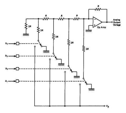
A DAC may consist of a series of Op amps for input for which
the gains have been selected to provide an output as given by the transfer
function. The most common variety however uses a resistive ladder network to
provide the transfer function.
Data Output Boards
Computer boards are available to plug right into your
personal computer expansion slot, providing digital-to-analog conversion,
address decoding and bus interfacing. In most cases, a supplier of the board
also provides software often written in C, BASIC, or assembly language to use
the board for data output.
2.3.3 Analog-to-Digital Converters (ADCs)
Sensors are devices that measure analog quantities, and
normally give an analog output, although techniques are available to convert
some sensor outputs directly into a digital format. The output from most
sensors is converted into a digital signal using an ADC. A digital number can
represent the amplitude of an analog signal, as previously stated. For
instance, an 8-bit word can represent numbers up to 256, so that it can
represent an analog voltage or current with an accuracy of 1 in 255 (one number
being zero). This assumes the conversion is accurate to 1 bit, which is
normally the case, or 0.4 % accuracy. Similarly, 10-bit and 12-bit words can
represent analog signals to accuracies of 0.1% and 0.025%, respectively.
Commercial integrated ADCs are available for instrumentation
applications. Several techniques are used for the conversion of analog to
digital signals, including: flash, successive approximation, resistor ladders,
ramp, and dual slope techniques.
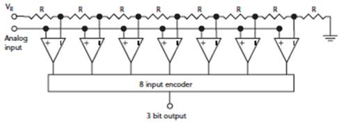
Flash converters are the fastest technique for converting
analog voltages into digital signals. The device basically consists of a series
of comparators (typically 255), biased to decreasing reference voltages as they
go lower down the chain. This concept is shown in the figure below for an 8-bit
converter, where only seven comparators are required, since a converter is not
needed for 0V. The comparators give a “0” output when the analog voltage is
less than its reference voltage, and a “1” output when the analog voltage is
higher than its reference input voltage. These outputs are then encoded to give
a 3-bit digital word. The devices are very fast, but expensive and with limited
applications. A number of flash converters are commercially available,
including the 8-bit flash converter manufactured by Maxim (MAX 104), which
gives a resolution of +/- 0.39% with an output sample rate of 1 GSPS (109
samples per second).
Minimum and Maximum Voltages
If a sensor has an output over a range, we must ensure that
the resulting digital value also varies over the same range with adequate
resolution to meet the specifications.
Bipolar Operation
Bipolar operation means that the binary number can represent
an input range from a negative value to a positive value. Usually though, the
most negative input value is represented by all zeros while the most positive
input value is represented as the maximum binary value.
ADC Characteristics
1.
Analog voltage input. This is the input voltage.
2.
Power supplies. Bipolar power supplies are
required for internal Op Amps.
3.
Reference voltage. This voltage is a regulated
voltage standard.
4.
Digital outputs. The converter will have output
lines representing the digital values.
5.
Control lines. The control lines allow for
interface with a digital computer.
6.
Conversion time. The ADC does not produce the
digital output instantaneously; therefore, propagation delay is introduced and
the computer must call for the digital data when it is ready.
ADC Structure
Most ADC's are available in the form of integrated circuit
assemblies.
Parallel Feedback ADC
A parallel feedback ADC uses a comparator and a D-to-A
converter with feedback to arrive at an analog value by trial and error until a
value is reached within the minimum resolution. When the logic counting network
determines the value is reached, the conversion is finished.
Ramp ADC
A Ramp-up or Stepped-up ADC is a low-speed device that
compares the analog voltage to a ramp voltage generated by an integrator or a
resistor network, as in a DAC. The voltage is ramped up, or stepped up, until
the voltage from the DAC is within the resolution of the converter. When it
equals the input voltage, the steps are counted, and the digital word count
represents the analog input voltage. This method is slow, due to the time
required for high counts, and is only used in low-speed applications. The
device is a medium cost converter. A 12-bit device has a conversion time of
approximately 5 ms.
Conversion Time Consequences
The finite conversion time of the ADC has serious
consequences on the rate of change of signals presented for conversion. If an
ADC is referring back to the input signal, which may be constantly changing, it
becomes obvious that errors will occur. Therefore, the answer is to hold the
input value constant during the process. This is accomplished with a
sample-and-hold circuit.
Sample-and-Hold
The basic concept of the sample-and-hold circuit is to place
it at the input of an ADC. When an electronic switch is closed, the capacitor
voltage will track the input voltage. At some time when a conversion of the
input voltage is desired, an electronic switch is opened, isolating the
capacitor from the input. Therefore, the capacitor will hold the voltage
applied by the switch. This voltage can then be converted to a digital value.
Practical S/H Issues
There are several practical issues associated with the
nonideal electrical characteristics of the elements involved in sample-and-hold
circuits. The sample-and-hold circuit typically uses an FET as the electronic
switch. The capacitor in combination with the “on” resistance of the FET create
a low pass filter with a critical frequency of operation. Therefore, the
sample-and-hold circuit may be limited in its update rate. Commercial
sample-and-hold circuits reduce this limitation by using a voltage follower
before the switch or FET since it has a very low output resistance.
Microprocessor Compatible ADCs
Data from ADCs must also be communicated to microprocessors.
This is typically done using tri-state output buffers on the ADC connected to
the computer data bus.
2.2.4 Frequency Based Converters
There's another important method by which an analog sensor
signal can be converted into a digital signal. This is based upon converting
the sensor signal into a variable frequency and then using this frequency as
input to a counter for a fixed interval of time. The output of the counter is
then a measure of the frequency and thus the sensor signal.
An alternative to the ADC is the voltage to frequency
converter. After the analog voltage is converted to a frequency, it is then
counted for a fixed interval of time, giving a count that is proportional to
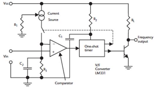
the frequency and the analog signal. Commercial units, such as the LM331 shown
in the figure below, are available for this conversion. These devices have a
linear relation between voltage and frequency. The operating characteristics of
the devices are given in the manufacturer’s data sheets. The comparator
compares the input voltage to the voltage across capacitor C2. If the input
voltage is larger, then the comparator triggers the one-shot timer. The output of
the timer will turn On the current source, charging C2
for a period of 1.1C1R2, making the voltage across C2 higher than the input
voltage. At the end of the timing period, the current source is turned Off, the
timer is reset, and C1R2 is discharged. The capacitor C2 will now discharge
through R3 until it is equal to the input voltage, and the comparator again
triggers the one-shot timer, starting a new cycle. The switched current source
can be adjusted by R1.
2.4 Data Acquisition Systems
The central processor is required to interface with a large
number of sensors and to drive a number of actuators. The processor has a
limited number of input and output ports, so that the data has to be channeled
into the input ports via external units, such as multiplexers, and channeled
out via demultiplexers to be distributed to the external actuators. The
multiplexers work by time division multiplex. For instance, an 8-bit
multiplexer will accept eight inputs, and output the signals one at a time
under process control.
ADC and Sample-and-Hold
The sample-and-hold circuit and ADC perform the actual
conversion.
Analog Multiplexer
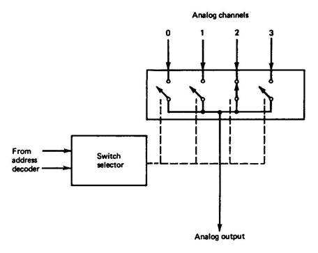
A 4-bit analog multiplexer is shown in the figure below. The
analog input signals can be alternately switched by CMOS analog switches to the
output buffer, similar to a rotary switch. A decoder controls the switches. The
decoder has input enables and address bits. When the enables are 0, all the
outputs from the decoder are 0, holding all of the analog switches Off. When
the enables are 1, the address bits are decoded, so that only one of the
control lines to the analog switches is a 1, turning the associated switch On
and sending the signal to the output buffer. The output from the multiplexer is
fed to the controller via an ADC. Analog multiplexers are commercially
available with 4, 8, or 16 input channels to 1 output channel, such a device is
the CD 4529. Analog demultiplexers are also commercially available.
Address Decoder Command Processor
The address decoder and command processor provide the data
to and from the processor at either specified time samples or by interrupt.
DAC and Latch
For output purposes the decoder and command processor are
used to latch data written to the DAS, which is then converted to an appropriate
analog signal by the DAC.
2.4.2 DAS Software
The process of selecting a channel in initiating a data
input from that channel involves some interface between the computer and a data
acquisition system. This interface is facilitated by software.
2.5 Characteristics of Digital Data
The conversion from analog-to-digital data results in a loss
of knowledge about the value of the variable.
2.5.1 Digitized Value
With digitized data there's a finite resolution of the
physical data represented by one part in. Therefore,
there may be a loss in value due to resolution.
2.5.2 Sampled Data Systems
Since the computer only takes periodic samples of the
variable, we lose some of the knowledge of the value relative to time.
Sampling Rate
The sampling rate determines how well the digital value
exactly tracks the analog value. If the sampling time is too long (the sampling
rate is too small), not enough information will be recorded digitally to
replicate the analog signal. In such a case, an altogether different signal
representation may result; this is called aliasing.
2.5.3 Linearization
In many cases, the input binary number and the control
variable are not linearly related. It is necessary to execute a program to
linearize the binary number such that it is proportional to the control
variable value.
Linearization by Equation
When the equation is known that relates the value of the
control variable and the binary number in the computer, an equation can be
developed to determine the linearized value of the variable.
Linearization by Lookup Table
It may not be possible to find a simple equation that relates the input variable with a linear output. In this case, a lookup table may be used. A lookup table may be accomplished by using software and reiterative calculation to arrive at some value from a table.