Electronics I – Week #3 Lab 1
Bridge Rectifier
Introduction:
Week 3 lab is based on the
previous lab from week 2 on half-wave and full-wave rectifiers and taking that
knowledge to build a bridge rectifier.
Materials and Equipment:
Materials:
·
Simulated Parts (Multisim):
· Two 2.2 kΩ resistors
Equipment:
·
Virtual Instruments
(Multisim):
· Agilent Multimeter
·
Agilent Function generator
Procedure:
*** This lab has to be implemented
only in software (running simulations on Multisim) ***
1.
Construct the bridge rectifier circuit shown in Figure 1. Notice that no
terminal of the transformer secondary is at ground potential (some simulation
software will not run if it is not connected to
the ground, check yours). The input voltage to the bridge, VSEC, is not
referenced to ground. Make sure to include resistor tolerance of 5%.
2.
Use a function generator to provide VAC and
run the simulation.
3.
Use a multimeter to measure VSEC (rms) and then use the
oscilloscope to measure the peak output voltage (VLOAD) without a filter capacitor.
Tabulate all data gathered.
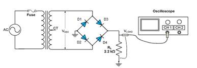
Figure 1
4.
Connect the
100 μF capacitor in
parallel with the load resistor. Measure VLOAD, the peak-to-peak ripple
voltage VRIPPLE,
and the ripple frequency. Tabulate all data gathered and compare the results
with and without the filter capacitor.
|
|
Without
the capacitor |
With
the capacitor |
|
Output
load voltage VLOAD |
|
|
|
Peak-to-peak
ripple voltage VRIPPLE |
|
|
|
Ripple
frequency |
|
|
5.
Choose a diode among the four connected to the bridge and open it. Simulate an
open diode in the bridge and explain what happens to the output voltage, the
ripple voltage and the ripple frequency?
6.
Investigate
the effect of the load resistor on the ripple voltage by connecting a second
2.2 kΩ, 5% tolerance,
and load resistor in parallel with RL and
C1 in the full-wave circuit of Figure 3. Measure
the ripple voltage. Captures a screenshot.
1. Compare a bridge rectifier
circuit with full-wave rectifier center-tapped circuit which you did in Lab 2.
Which circuit has the higher output voltage?
2. Explain how you could measure
the ripple frequency to determine if a diode were open in a bridge rectifier
circuit.
3. What is the maximum dc voltage you could expect to
obtain from a transformer with a 3 Vrms secondary
using a bridge circuit with a filter capacitor?
1. Measure the voltage VSEC and the output load voltage, VLOAD without a filter capacitor. Capture
the screenshots of your measurements.
2. Measure the output load
voltage, VLOAD,
with the capacitor and the peak-to-peak ripple voltage, VRIPPLE, in the output. Capture the screenshots of your measurements.
Also, measure the ripple frequency. Table with all the data gathered for the
circuit with and without the capacitor.
3. Follow the template “Lab
Report Template” to compile the report and make sure to check the report
against the grading rubric below. The template can be found in the “Tools and
Templates” link in the navigation center.
4. Make sure to include the
table, calculations, screenshots of
the measurements and the answer to the questions. Save the document as Lab2YourGID.docx (ex: Lab3G00000000.docx).
Rules for lab
submissions:
1.
The lab document must be a Word document.
PDF files are NOT accepted.
2.
All screenshots must be included.
3.
All Multisim screenshots must include
the date/time stamp. See TOOLS AND TEMPLATES for the procedure to display
the date and time.
4.
Any and all Multisim files must be
submitted.
5.
Any equations used must be typed in
Word. Copy and paste of equations from outside sources is
prohibited.
6.
No graphics are allowed in the Word document
other than screenshots of circuits from Multisim and hardware if applicable,
with the date/time stamp.
7.
The lab template should be used.
Specifically, it is brought to your attention that a summary MUST be provided
explaining the results of the labs, the relationship of the results to expected
results, and any challenges encountered.
8.
Hardware portion of labs should include
screenshots of the assembled circuit with your name and student GID number
written on paper next to the circuit. There should be screenshots of the
instrument readings with the date and time stamp on lower right corner clearly
shown.
Any violation of the submission rules above will
result in a grade of 1.
|
Grading Criteria |
Points |
|
Construct
bridge rectifier circuit in Multisim without a capacitor |
15 |
|
Measurement
of VSEC and VLOAD voltages with screenshots |
10 |
|
Construct
bridge rectifier circuit in Multisim with a capacitor |
10 |
|
Measurement
of VSEC,
VLOAD and VRIPPLE voltages with screenshots |
15 |
|
Simulation
with an open diode and measurement with screenshots |
20 |
|
Including
5% tolerances in the measurements |
10 |
|
Review
Questions |
10 |
|
Report
format (Proper use of template) |
10 |
|
TOTAL |
100 |
![]()