Electronics I – Week #1 Lab 1
Semiconductors and Diode Theory
Please Note: If you need help with your labs,
please don't hesitate to reach out to the tutoring center ASAP. They have
lots of good resources and are available to work with you to be
successful.
Introduction:
Welcome to the first lab in
ET212. Week 1 lab is an introduction to semiconductors and diode theory and
should be implemented in software (Multisim) only. Week 2 onwards labs will be
implemented in hardware only using NI myDAQ development
tool, software only or both.
·
For instructions on setup and installation of NI myDAQ hardware and software, please review the
documents “Setting up NI myDAQ” and “Installation and Activation of
NI myDAQ”.
NOTE: THE MYDAQ SOFTWARE IS A DOWNLOAD ONLY. DVDs ARE NO LONGER SHIPPED
WITH THE HARDWARE KIT.
·
Once you receive the hardware kit, review the contents and
install the software: Multisim, NI LabVIEW and NI ELVISmx.
Watch the video “Video : Tour of the NI ELVISms Instrument launcher”.
·
Complete the Safety Module.
Materials and Equipment:
Materials:
· Simulated Parts (Multisim):
1N4001 Diode
Two resistors
(2.2 KΩ and 1.8 KΩ)
Equipment:
· Virtual Instruments (Multisim):
Agilent
Multimeter
Procedure:
** This lab has to be implemented
only in software (running simulation in Multisim) **
1.
Construct the circuit shown in Figure 1 below in Multisim with
R1 = 2.2 KΩ and R2 = 1.8 KΩ. Use a 10% tolerance for the resistors.
Assume an ideal diode.
Part A:
1.
Calculate current ‘I’ in the circuit shown in Figure 1. Show work.
2.
Calculate the voltage drops across R1 and across R2.
3.
Construct the circuit in Multisim and measure the current in the circuit using
the Agilent Multimeter. Compare it to your calculated value in Step 1.
4.
Using the Agilent Multimeter, measure the voltage drops across R1 and across
R2, and compare it to what you calculated in Step 2.
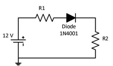
Figure 1
Part B:
1.
Reverse the polarity of the diode and analyze the circuit. Repeat steps 1) and
2) from Part A.
2.
Construct the revised circuit in Multisim and repeat steps c) and d) from Part
A.
3.
Tabulate all your data below using appropriate units. Be sure to capture the
screen for the measured values.
Table 1:
|
|
Calculated |
Measured |
|
Part
A: Current (I) |
|
|
|
Part
A: Voltage drop across R1(VR1) |
|
|
|
Part
A: Voltage drop across R2 (VR2) |
|
|
|
Part
B: Current (I) |
|
|
|
Part
B: Voltage drop across R1 (VR1) |
|
|
|
Part
B: Voltage drop across R2(VR2) |
|
|
Review Questions:
1.
Does the simulation results match the calculated values? If not, explain what
causes this difference in the measurements.
2.
What is the difference between Part A and Part B with respect to the current
and voltage drop in the circuit?
Deliverables:
1. Follow the template “Lab
Report Template” to compile the report and make sure to check the report
against the grading rubric below. The template can be found in the “Tools and
Templates” link in the navigation center.
2. Make sure to include the
table, calculations, screenshots of the measurements and the answer to the
questions. Save the document as Lab1YourGID.docx (ex: Lab1G00000000.docx).
Rules for lab
submissions:
1. The lab document must be a Word document. PDF files are NOT accepted.
2. All screenshots must be included.
3. All Multisim screenshots must include the date/time stamp. See TOOLS AND TEMPLATES for the procedure to display the date and time.
4. Any and all Multisim files must be submitted.
5. Any equations used must be typed in Word. Copy and paste of equations from outside sources is prohibited.
6. No graphics are allowed in the Word document other than screenshots of circuits from Multisim and hardware if applicable, with the date/time stamp.
7. The lab template should be used. Specifically, it is brought to your attention that a summary MUST be provided explaining the results of the labs, the relationship of the results to expected results, and any challenges encountered.
8. Hardware portion of labs should include screenshots of the assembled circuit with your name and student GID number written on paper next to the circuit. There should be screenshots of the instrument readings with the date and time stamp on lower right corner clearly shown.
Any violation of the submission rules above will result in a grade of 1.
Grading Rubric:
|
Grading
Criteria |
Points |
|
Part
A: Analyze the circuit to calculate the current (I) |
10 |
|
Part
A: Analyze the circuit to calculate the voltage drop across R1 and R2 (VR1
and VR2) |
10 |
|
Part
A: Construct the circuit and run the simulation to measure the current and
voltage drop across R1 and R2 |
15 |
|
Part
B: Analyze the circuit to calculate the current (I) |
10 |
|
PartB: Analyze the circuit to calculate the voltage drop
across R1 and R2 (VR1 and VR2) |
10 |
|
Part
B: Construct the circuit and run the simulation to measure the current and
voltage drop across R1 and R2 |
15 |
|
Including
5% tolerances in the measurements |
10 |
|
Table
and Review Questions |
10 |
|
Report
format ( Proper use of template) |
10 |
|
TOTAL |
100 |
![]()